
How to Prevent Delamination in Coverlay PCB
Prevent Delamination in Coverlay PCB
The flexible printed circuit board’s copper traces, pads, and other components require protection from external factors like dust, moisture, chemicals, and mechanical stresses. This is why FPC coverlay is a crucial component of any flexible PCB. It protects the conductor layers from environmental factors and ensures that the copper traces, pads, and other components will remain intact during flexing, folding, and twisting.
Coverlay is a layer of polyimide or another dielectric that’s bonded to the surface of a flex circuit board to protect the conductor layers and prevent damage to them. The coverlay also helps improve the flex circuit’s electrical properties and adds insulation. While it does require additional processing steps – surface treatment, adhesive application, lamination, and trimming – it’s worth the extra time for its durability, reliability, and flexibility benefits.
While the benefits of coverlay are many, there are some problems associated with it. Two of the most common issues are measling and delamination. Measling is characterized by circular white spots on the flexible circuit’s interior weave that are the result of stress and production processes. It isn’t a major concern for most PCBs, but it does indicate that there may be underlying defects that need to be addressed. Delamination, on the other hand, is a partial separation of the layers of your circuit board that leads to gaps or blisters in the layers. It can be the result of unwanted heat, humidity, or stress during manufacturing, and it’s a serious concern because it can ruin your circuit boards.
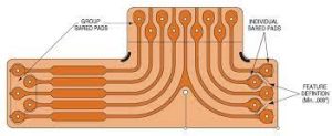
How to Prevent Delamination in Coverlay PCB
Both measling and delamination can be avoided by using the proper materials, ensuring that the manufacturing process is meticulously controlled, and using an adequate amount of adhesive. It’s also important to choose the right coverlay thickness based on your circuit board’s temperature requirements. The stiffeners can be made from a variety of materials, including polyimide and FR-4. However, it is important to choose the right material for your project to prevent any long-term failures.
Another issue is air bubbles and voids in the coverlay pcb film that are caused by poor surface preparation, contamination, and weak adhesives. These problems can result in cracked coverlay that affects the PCB’s dielectric characteristics. The voids and bubbles can be a pain to deal with, but it’s not impossible to resolve them by adding more adhesive.
Finally, delamination can occur between the flex circuit and FR4 stiffener if the parts are not properly dried before assembly. The absorbed moisture can convert to steam during the reflow soldering operation, which causes the layers of the flex circuit and stiffener to separate. This problem can be prevented by pre-baking the flex and rigid-flex components prior to assembly and limiting the time they’re exposed to the ambient environment.
Before applying the coverlay, the PCB design must be finalized. This includes determining the layout, routing, and the areas where the coverlay will be applied. The design should specify the openings in the coverlay for pads, vias, and other contact points. The preparation phase also includes selecting the appropriate coverlay material, typically polyimide film with an adhesive layer, based on the requirements of the PCB.